Wave Optics Module

Analyze Micro- and Nano-Optical Devices

The Wave Optics Module, an add-on to the COMSOL Multiphysics® software platform, is used by engineers and scientists to understand, predict, and study electromagnetic wave propagation and resonance effects in optical applications. By analyzing electromagnetic field distributions, transmission and reflections coefficients, and power dissipation in a proposed design, simulation of this kind leads to more powerful and efficient products and engineering methods.

In order to optimize designs for photonic devices, integrated optics, optical waveguides, couplers, fiber optics, and more, you need to account for real-world scenarios. The multiphysics modeling capabilities of the COMSOL Multiphysics® software help you study how other physics affect optical structures; for instance, stress-optical, electro-optical, and acousto-optical effects as well as electromagnetic heating.

Contact COMSOL
An optical ring resonator model showing the  electric field in the Rainbow color table.

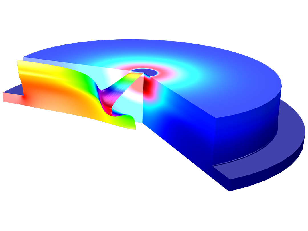
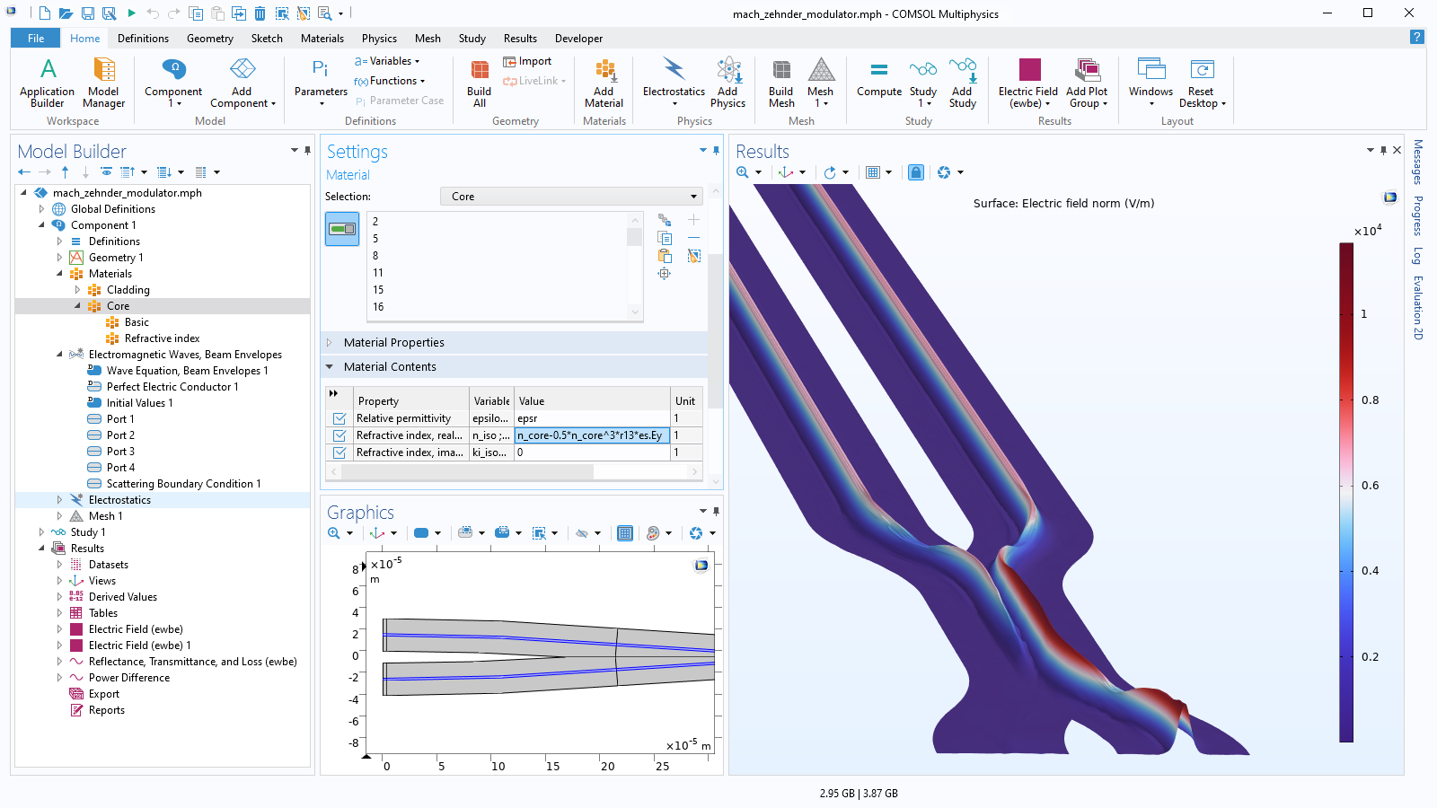
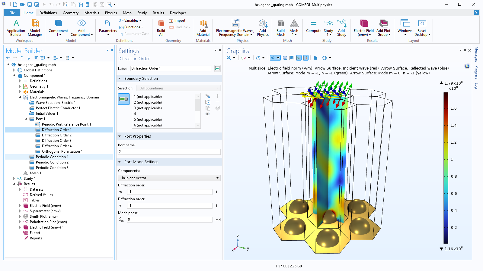
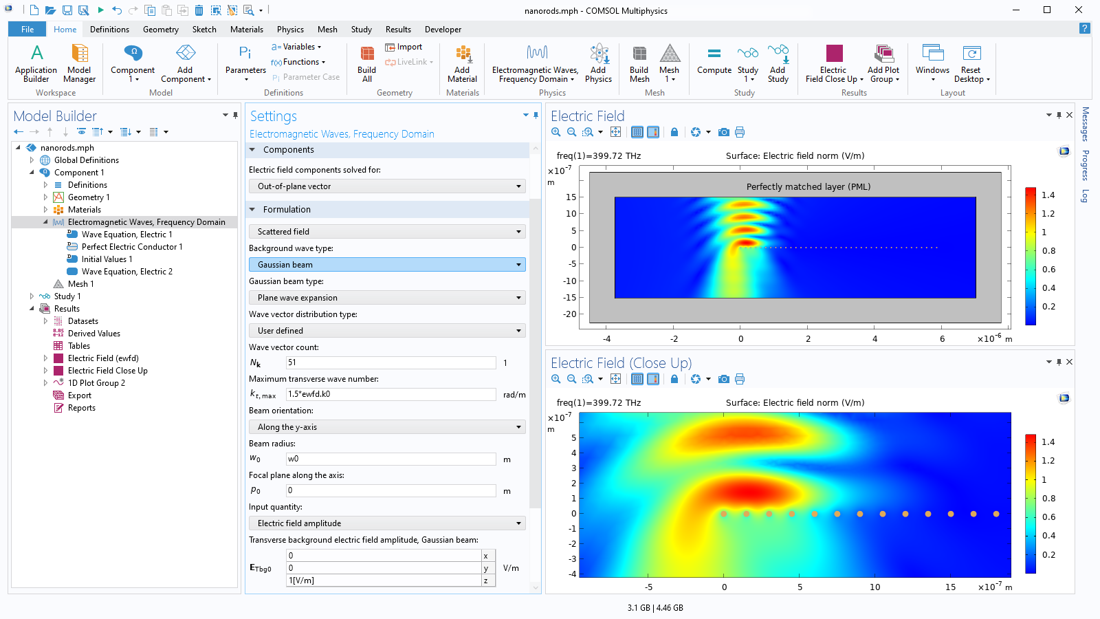
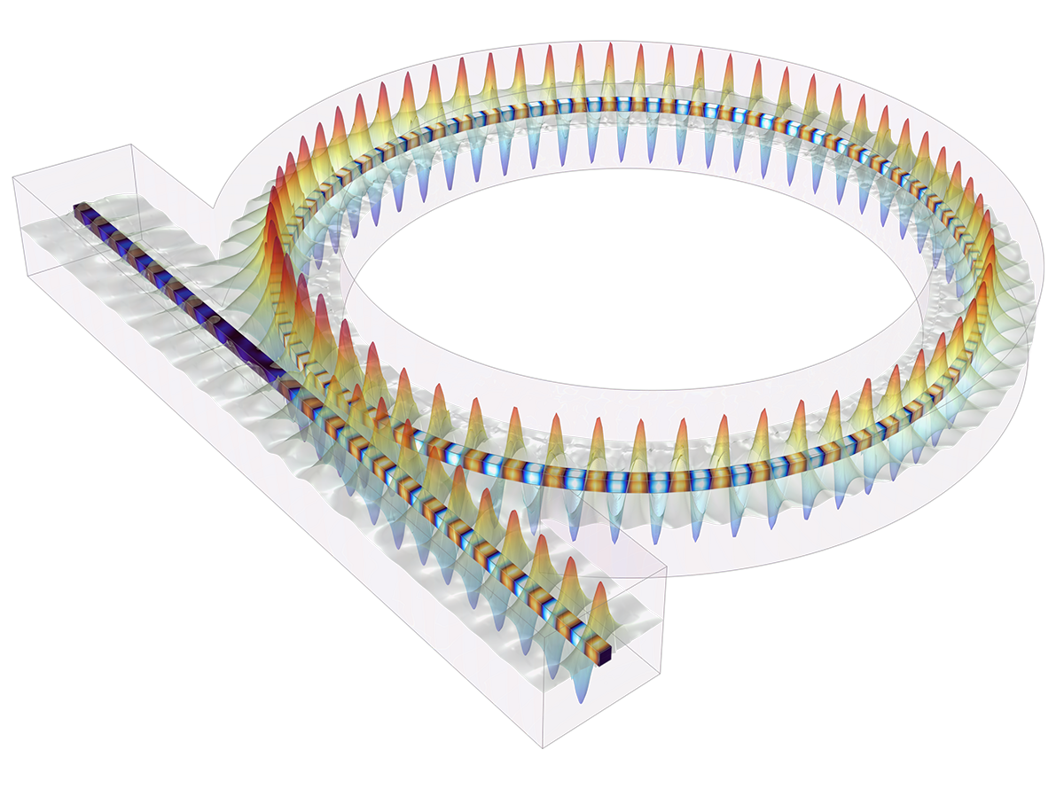
Model Optically Large Problems with the Beam Envelope Method

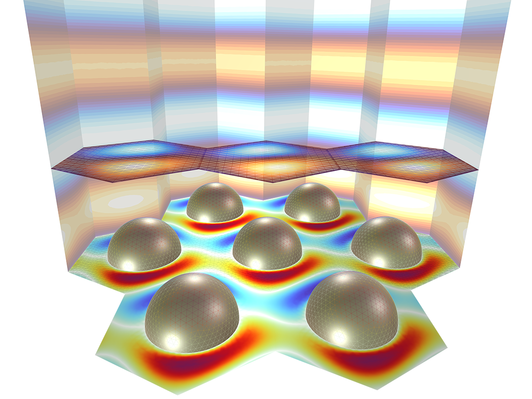
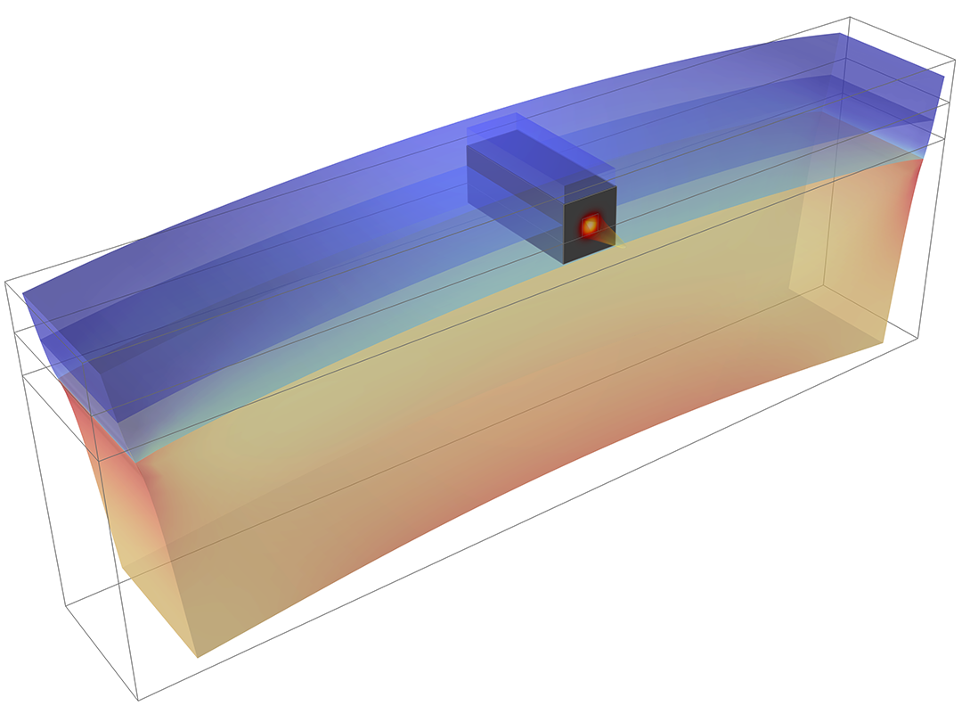
In addition to traditional numerical methods, the Wave Optics Module includes a specialized beam envelope method that can be used to simulate optically large devices with far fewer computational resources than conventional techniques. Applications include directional couplers, fiber Bragg gratings, lens systems, waveguides, external optical systems, fiber couplings, laser diode stacks, and laser beam delivery systems.

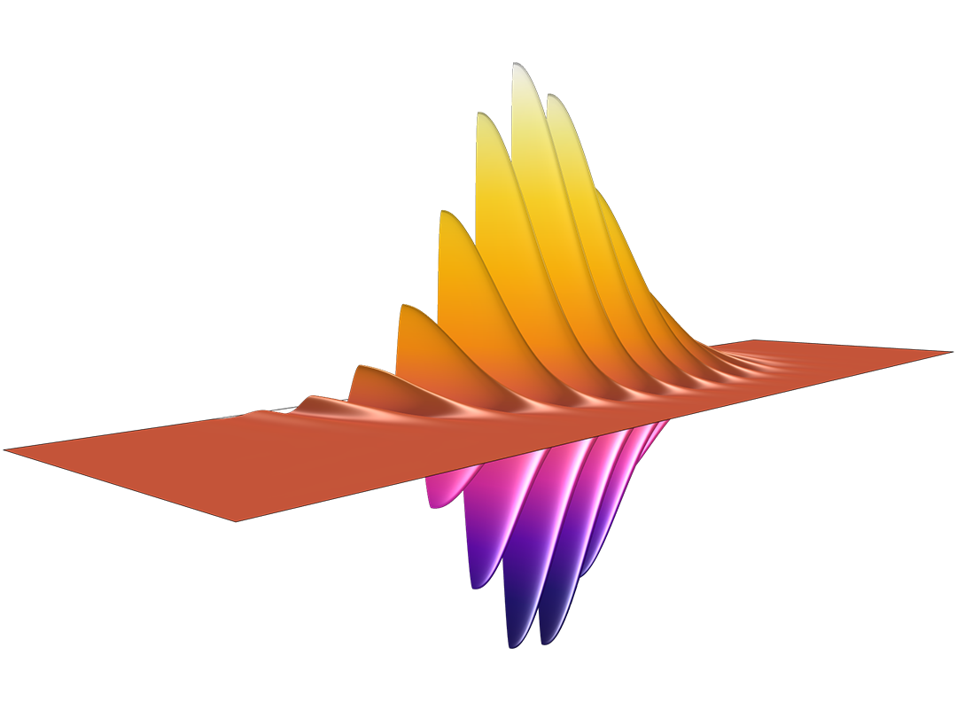
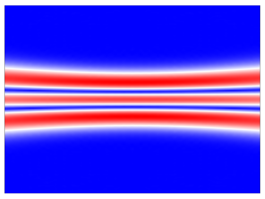
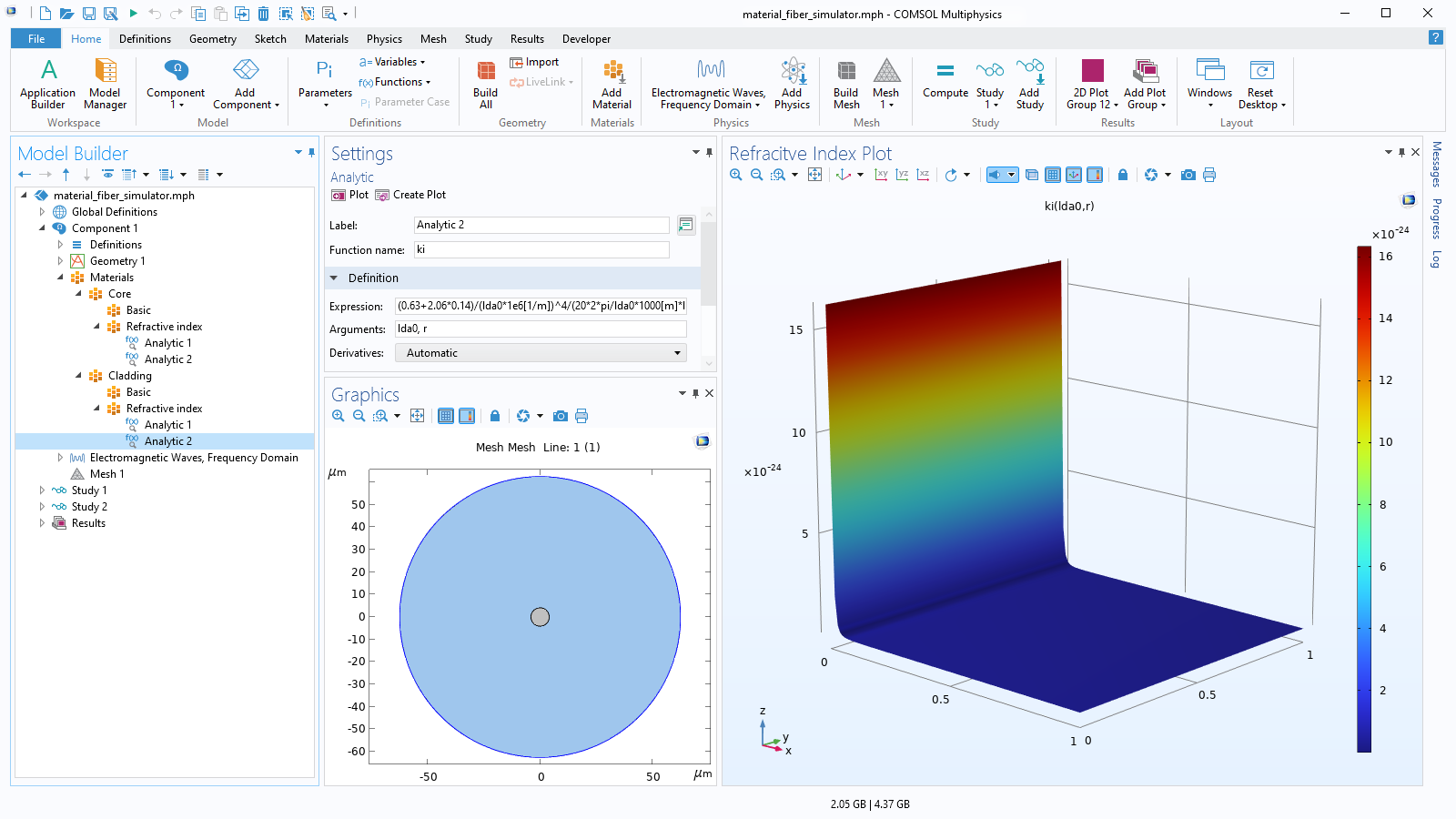
The beam envelope method analyzes the slowly varying electric field envelope for optically large simulations without relying on approximations. It requires much fewer mesh elements to resolve each propagating wave when compared to traditional methods.


What You Can Model with the Wave Optics Module

Perform various optics analyses with the COMSOL® software.

A closeup view of an optical fiber model showing the electric field.

Optical Fibers

Mode analysis and wave propagation in optical fibers.

A closeup view of a beam model showing the spiraling phase distribution.

Propagation of Beams

Gaussian or plane wave propagation in dielectrics or free space.

A closeup view of a  Gaussian beam model propagating through a light guide, visualized in a zig-zag pattern.

Waveguides

Computation of transmission and reflection coefficients of waveguides.

A close-up view of two directional coupler models showing the electric field.

Waveguide Couplers

Analysis of the field coupling between waveguides in close proximity.

A closeup view of a gold nanosphere model showing the optical scattering.

Optical Scattering

Scattering of plane waves and Gaussian beams.

A closeup view of a wire grating on a dielectric substrate showing the electric field norm.

Plasmonics

Electromagnetic excitations of surface plasmons and plasmon polaritons.

A closeup view of a photonic crystal model showing the electric field.

Photonic Crystals

Photonic crystals and bandgap structures.

A closeup view of a laser beam model showing the second harmonic generation.

Nonlinear Optics

Second harmonic generation, self-focusing effects, and other nonlinear effects.

A closeup view of a laser cavity model showing the electric field.

Laser Cavities

Resonant frequencies and threshold gain of laser cavities.

A closeup view  hexagonal grating model with seven protruding semispheres.

Gratings and Metamaterials

Transmission, reflectance, and diffraction of gratings, metamaterials, and general periodic structures.

A closeup view of a photonic waveguide model showing the electric field.

Stress-Optical Effects1

Effects of stress-induced birefringence in waveguides.

A closeup view of an LED device showing the electroluminescence emission rate.

Optoelectronics2

Emission, absorption, and refractive index changes in optoelectronic devices.

  1. Requires the Structural Mechanics Module or MEMS Module
  2. Requires the Semiconductor Module

Features and Functionality in the Wave Optics Module

Explore the features and functionality of the Wave Optics Module in more detail by expanding the sections below.

A closeup view of the Model Builder with the Electromagnetic Waves, Beam Envelopes node highlighted and a Fresnel lens model in the Graphics window.

Full-Wave Electromagnetics Analyses

The Wave Optics Module enables you to quickly and easily set up a model in 2D, 2D axisymmetric, and 3D domains. Both fundamental and advanced boundary conditions are included for your analyses.

The workflow is straightforward and can in general be described by the following steps: create or import the geometry, select materials, select a suitable Wave Optics interface, define boundary and initial conditions, define the mesh, select a solver, and visualize the results. All of these steps are accessed from the COMSOL Multiphysics® environment. Meshing and solver settings are automatic with options for manual editing.

The functionality of the Wave Optics Module covers simulation of electromagnetic fields and waves based on Maxwell’s equations together with material laws for propagation in various media. The modeling capabilities are accessed via built-in user interfaces, which allow you to analyze wave phenomena in optics and photonic devices.

The Wave Optics Module enables modeling in the frequency and time domain, including eigenfrequency, and mode analysis.

A closeup view of the Model Builder with the Analytic node highlighted and an optical fiber model in the Graphics window.

Optical Materials

Use materials from the built-in optical materials database or define your own. You can specify the relative permittivity or refractive index as well as include more advanced material properties such as Debye, Drude–Lorentz, and Sellmeier dispersion. Materials can be anisotropic as well as functionally graded.

Take full control over your simulation by modifying material definitions, the governing Maxwell's equations, or boundary conditions directly within the software. This flexibility enables you to create a variety of user-defined materials, including metamaterials, with engineered properties, and gyromagnetic and chiral materials.

A closeup view of the Surface node settings and a plasmonic wire grating model in the Graphics window.

Data Visualization and Extraction

The results are presented using, for example, plots of electric and magnetic fields, reflectance, transmittance, diffraction efficiency, S-parameters, power flow, and dissipation. You can also create visualizations of nonstandard expressions in terms of physical quantities that you can define freely. This makes it possible to gain deeper insight by enabling examination of virtually every aspect of the results.

A closeup view of the Model Builder with the Polarization node highlighted and a 1D plot in the Graphics window.

Nonlinear Optics

The Wave Optics Module provides several features for simulating nonlinear optics in both the time and frequency domains. In the frequency domain, you can have field-dependent material properties for phenomena such as self-focusing, or you can couple multiple frequency-domain analyses together to model mixing between two or more waves at different frequencies like sum or difference frequency generation. By incorporating nonlinear polarization terms, this approach allows for nonlinear simulations using continuous wave (CW) lasers or other quasi-steady-state phenomena. There is similar flexibility in the time domain, where polarization or remnant electric displacement terms can be modified to enable more advanced modeling scenarios like ultrafast phenomena.

A closeup view of the Model Builder with the Port node highlighted and a 2D model in the Graphics window.

Boundary Conditions

Electromagnetic wave modeling requires highly specialized boundary conditions, including the capability of modeling unbounded domains as well as periodic structures such as metamaterials. For example, modeling a periodic metamaterial requires periodic ports that can handle arbitrary angles of incidence and diffraction orders. For general modeling of waveguides and optical fibers, numerical mode-matched ports are required to properly feed waveguides with incoming light.

Important Boundary Conditions in the Wave Optics Module

  • Perfect electric conductor (PEC)
  • Impedance (finite conductivity)
  • Transition (thin lossy conductive sheet)
  • Periodic ports with arbitrary diffraction orders
  • Floquet, or Bloch, periodicity
  • Scattering (absorbing) boundaries
  • Ports
    • Analytical shapes
    • Numeric (mode matched)
A closeup view of the Model Builder with the Core node highlighted and a modulator model in the Graphics window.

Multiphysics Effects in Optical Devices

The Wave Optics Module can be combined with any other module to simulate multiphysics phenomena, all of which seamlessly integrate with the core COMSOL Multiphysics® software platform. This means that your modeling workflow remains the same, regardless of the application area or physics you are modeling.

You may want to examine the effects that mechanical deformation has on your device's performance, including stress-optical effects. Similarly, you can examine how heat transfer, thermal stress, and thermal dissipation affect a device.

Additionally, you can simulate how various physical phenomena can be used for modulation purposes, such as acousto-optical, electro-optical, and magneto-optical effects.

By combining with a mass transport simulation, you can compute realistic refractive index profiles with anisotropic diffusion coefficients and use the results in an electromagnetics analysis.

A closeup view of the Model Builder with the Diffraction Order node highlighted and a hexagonal grating model in the Graphics window.

Periodic Structures

Periodic structures are fundamental to many engineered electromagnetic structures being developed for applications such as polarimetric and subwavelength imaging and diffractive optics. In the Wave Optics Module, you can model these structures, including their high-order diffraction modes, with Floquet periodic conditions and varying diffraction orders. Using these features, you can accurately design elements for metasurfaces and other flat optics.

A closeup view of the Electromagnetic Waves, Frequency Domain node settings and two Graphics windows.

Scattering

Accurate scattering models of gold nanoparticles, for example, can be easily accomplished using a scattered field formulation. In this approach, the Wave Optics Module provides you with the choice of an incident plane wave, a Gaussian beam (both with and without the paraxial approximation), or a user-defined excitation and then solves for the scattered field induced by the chosen excitation. The simulation domain can approximate an infinite space by absorbing the outgoing radiation using perfectly matched layers (PMLs), which simultaneously absorb radiation for a range of frequencies and angles of incidence. Using a near-to-far field transformation, the far-field radiation of the scatterer can be analyzed.

Every business and every simulation need is different.

In order to fully evaluate whether or not the COMSOL Multiphysics® software will meet your requirements, you need to contact us. By talking to one of our sales representatives, you will get personalized recommendations and fully documented examples to help you get the most out of your evaluation and guide you to choose the best license option to suit your needs.

Just click on the "Contact COMSOL" button, fill in your contact details and any specific comments or questions, and submit. You will receive a response from a sales representative within one business day.

Next Step

Request a Software Demonstration