support@comsol.com
Semiconductor Module Updates
For users of the Semiconductor Module, COMSOL Multiphysics® version 6.2 provides easy preview of doping profiles prior to solving; significantly improved stability, accuracy, and efficiency for the finite-element-based physics interfaces; and substantial enhancements to the optoelectronics modeling workflow. Read more about the updates below.Preview Buttons for Visualizing Doping Profiles
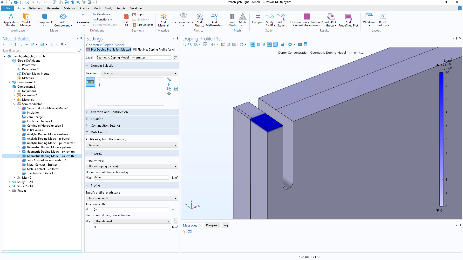
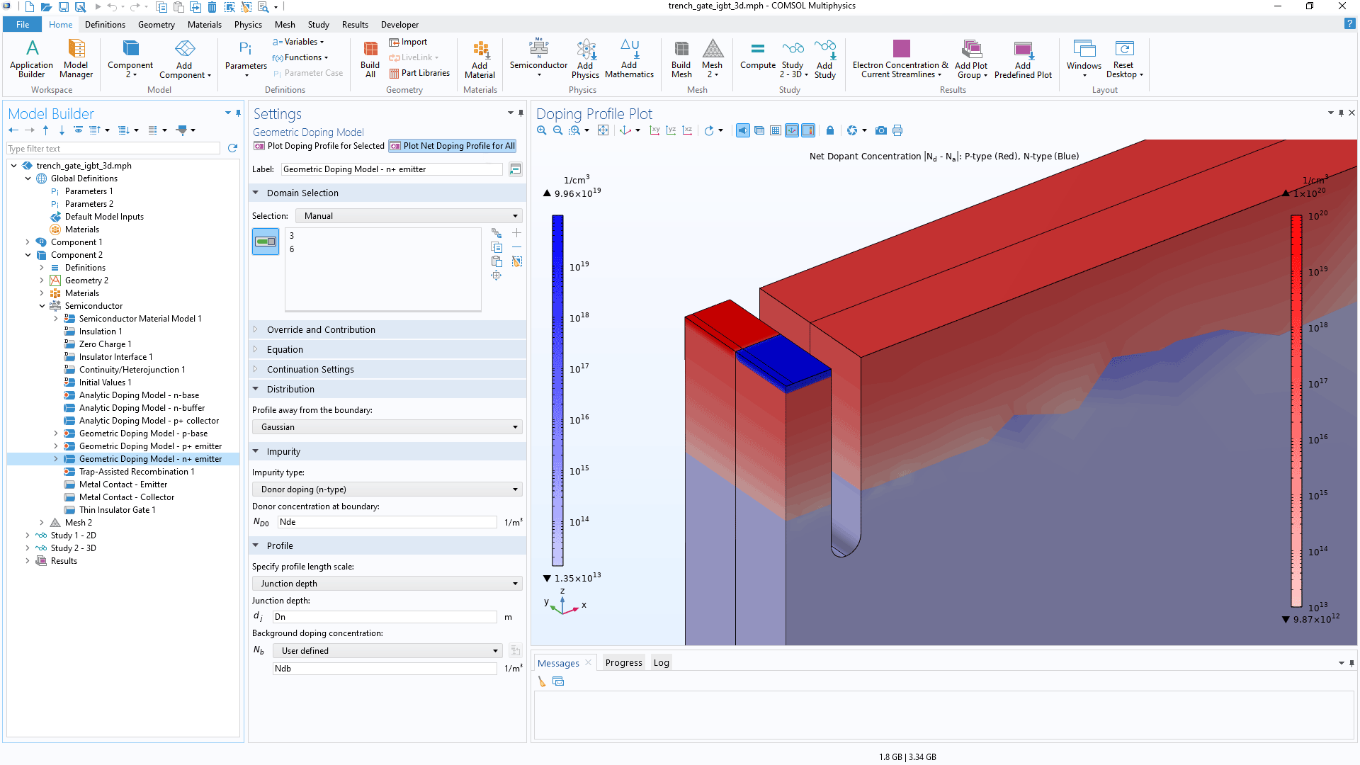
A precise doping profile definition is paramount in semiconductor modeling. There are two new preview buttons within the Analytic Doping Model and Geometric Doping Model features that can be used to visualize doping profiles prior to solving the model equations. The two preview buttons, Plot Doping Profile for Selected and Plot Net Doping Profile for All, are accessible within both the Settings window and the context menu. The Plot Doping Profile for Selected button can be used to visualize the dopant concentration introduced by the selected doping feature, whereas the Plot Net Doping for All button visualizes the absolute value of the net dopant concentration. For the net-doping profile plots, the p-type region is displayed in red and the n-type region is displayed in blue, making it easy to distinguish between the two and ensure that the model definition is correct before solving the equations. You can explore this new functionality with the following models:
- bipolar_transistor
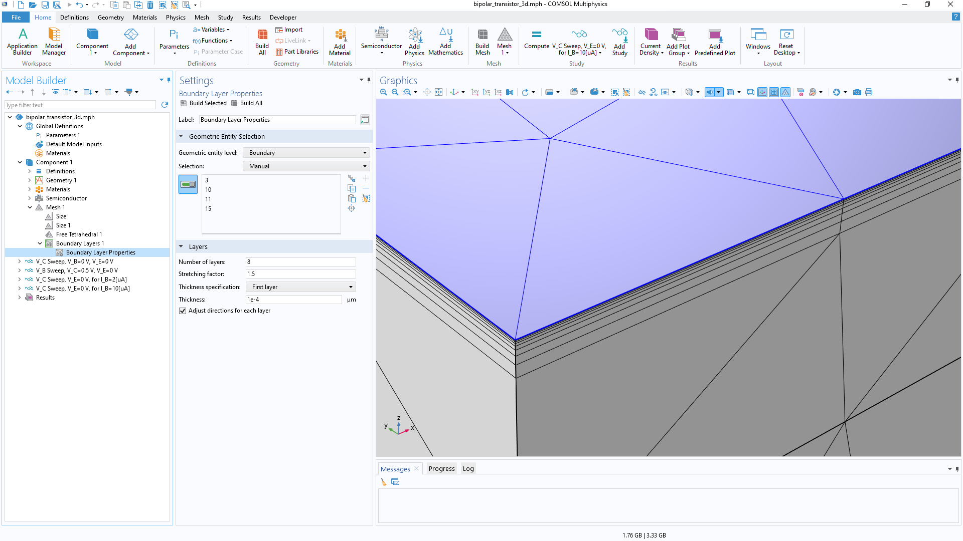
- bipolar_transistor_3d
- mosfet
- trench_gate_igbt_3d
- gaas_pn_junction_infrared_led_diode
Performance Improvements for Finite Element Formulations
Significant enhancements have been made to the stability, accuracy, and efficiency of finite element formulations, including logarithmic, quasi-Fermi level, and density-gradient formulations. These improvements encompass various aspects, such as improvements to weak-form equations, constraint settings, and default solver settings. As a result, a majority of the models in the Application Library can now be solved more efficiently using finite element formulations. For instance, previously, solving a 3D bipolar transistor model with the finite volume formulation typically took a full day, whereas with the improved finite element log formulation, this model can now be solved on a standard PC in 15 minutes.
Simplified Optoelectronics Modeling Workflow
Improvements have been made to the user interface for the optoelectronics modeling workflow, and the process for defining optical physics with the Semiconductor interface or through other optics interfaces has been streamlined. For the Semiconductor Electromagnetic Waves Coupling feature, an information message will now appear if optical physics are provided, and a schematic detailing of the coupling has been added to the Equation section in the Settings window.
Infinite Element Domain for Modeling Quantum Physics
An Infinite Element Domain feature can now be added to models that include the Schrödinger Equation interface. You can view this update in the new Solving the Hydrogen Atom tutorial model.
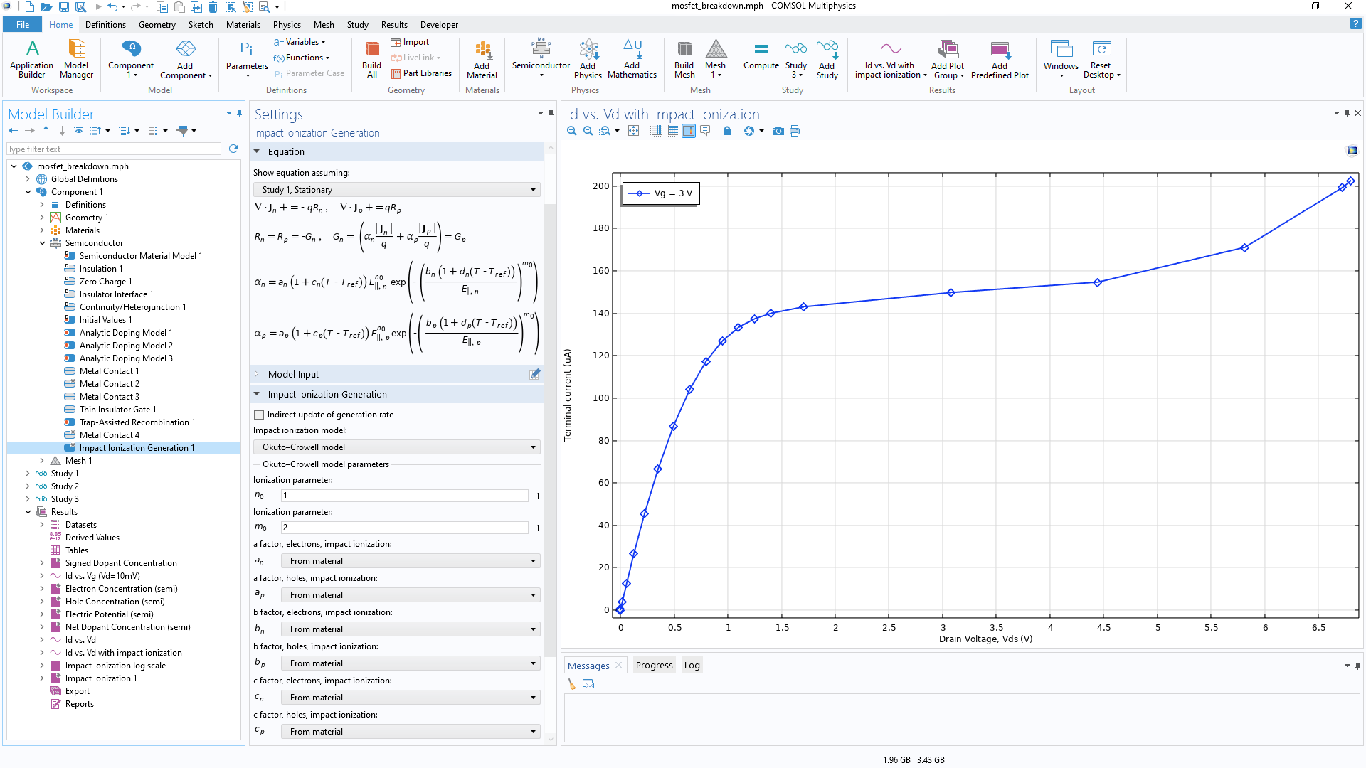
Extended Impact Ionization Generation Model
The Okuto–Crowell model in the Impact Ionization Generation feature has been updated to a more general expression that can account for different dependencies on an electric field using two additional ionization parameters.
New Default Plots Include Net Dopant Concentration
A default Net Dopant Concentration plot group has been added to the Semiconductor interface and will automatically display the absolute value of the net dopant concentration.
New and Updated Tutorial Models
COMSOL Multiphysics® version 6.2 brings the following new and updated tutorial models to the Semiconductor Module.
Electrolyte-Gated Organic Field-Effect Transistor
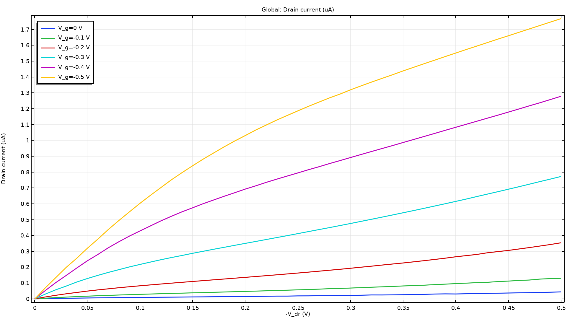
Application Library Title:
egofet
Download from the Application Gallery
Solving the Hydrogen Atom
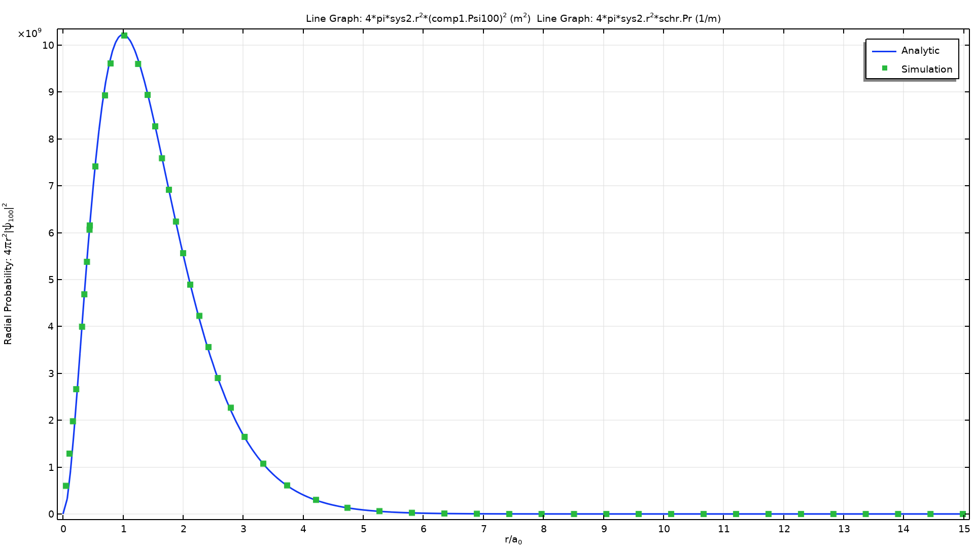
Application Library Title:
solving_hydrogen_atom
Download from the Application Gallery
Bipolar Transistor
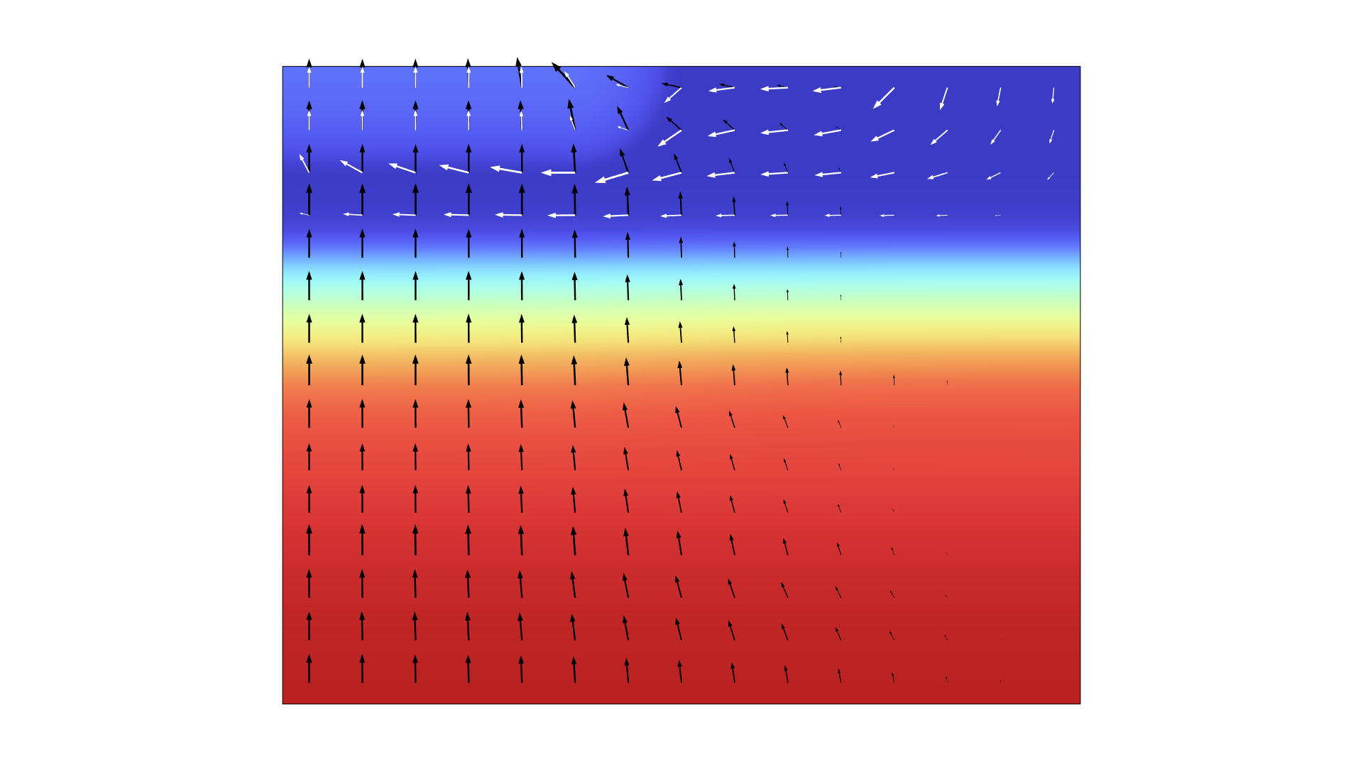
Application Library Title:
bipolar_transistor
Download from the Application Gallery
3D Analysis of a Bipolar Transistor
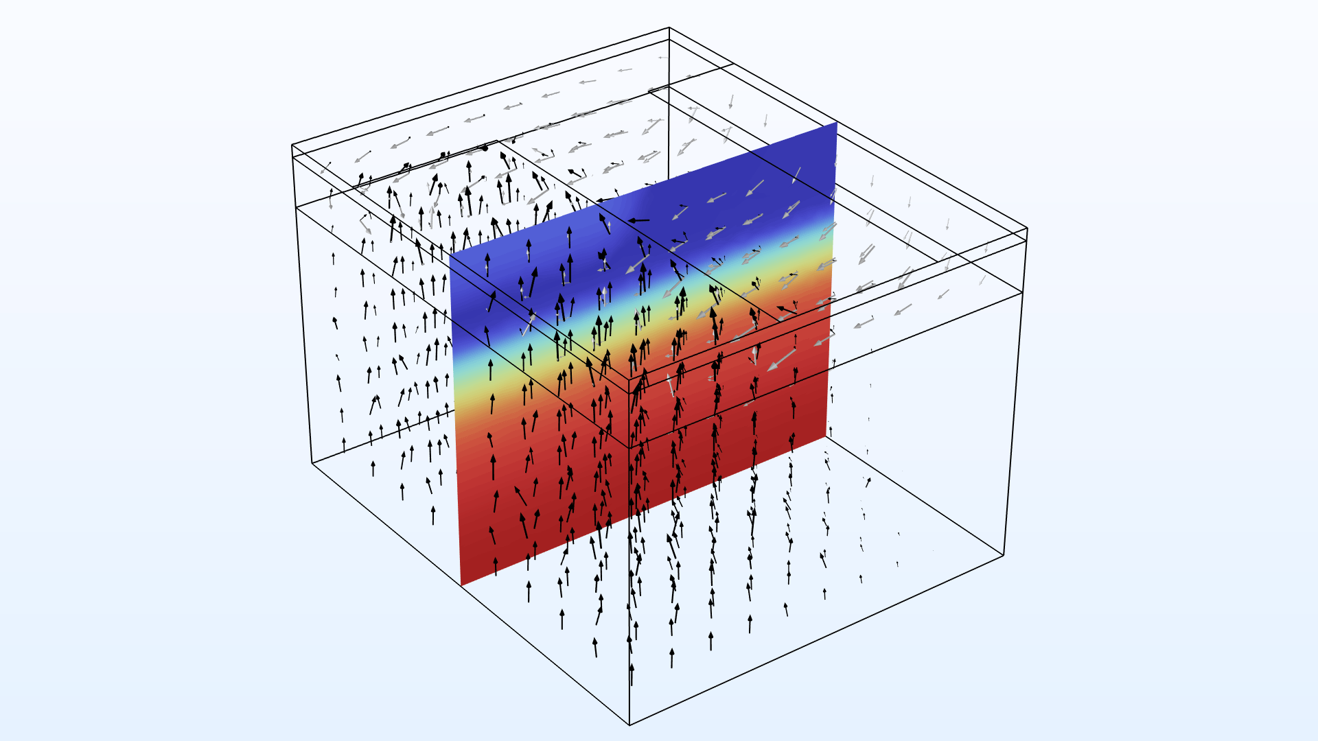
Application Library Title:
bipolar_transistor_3d
Download from the Application Gallery