Modeling Electrochemical Deposition of Aluminum from Ionic Liquids for PCB Applications
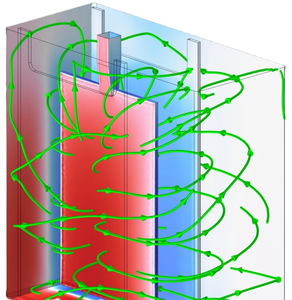
While copper remains the dominant material for conduction paths in printed circuit board (PCB) applications, both technological and economic reasons have been motivating research on substituting copper with aluminum (Al). Despite its 60 % higher specific electrical resistance, aluminum features twice the conductivity of copper per weight, enabling lighter weight applications where volume is no major constraint such as in aerospace technology. Electroplating is an established method for producing metallic layers and patterns on circuit board substrates. Here, an electric current is applied between the cathodic substrate and an anode, thus reducing the metal ions electrochemically and forming a metallic layer at the substrate surface. One major obstacle for wide spread usage of Al for PCB applications arises from its highly negative standard electrode potential, preventing electrochemical deposition from aqueous electrolytes. To address this property, ionic liquids (IL) – organic salts in liquid state at process temperature – mixed with Al salts can be utilized. While enabling electrochemical deposition of Al, these IL-based electrolytes bring another challenge regarding the coating of vias, which electrically connect both sides of the PCB substrate. In order to supply these through bores with fresh electrolyte, an additional convective flow has to be integrated into the electroplating process. Due to the physical properties of ILs, the dynamic viscosity of these electrolytes is one order of magnitude higher than that of aqueous electrolyte solutions, which results in unfavorable flow conditions. To increase electrolyte replacement within these vias, the PCB substrate is moved in a controlled manner between two opposing plate electrodes. To represent the electroplating process of Al on a PCB substrate containing vias by simulation, a two-stage modelling approach was developed and implemented in COMSOL Multiphysics®. In the first stage, fluid dynamics within the process chamber geometry (~1e-1 m) imported from CAD data were modelled in 3D. Here an unperforated PCB substrate is fully immersed into the IL and performing an oscillating motion between two electrode plates. This motion was implemented into the model using the Moving Mesh interface. As the IL is comparably viscous, the resulting electrolyte convection was computed using the Laminar Flow interface. The resulting pressure difference between the opposing surfaces of the substrate was integrated into the second stage of the modelling approach. In this stage, a 2D representation of a via (~1e-4 m) through the substrate was modelled utilizing rotational symmetry. Based on the pressure data of the macroscopic CFD model and a given current characteristic, this microscopic model was used to compute ion transport, Al deposition and the resulting layer geometry near the via. Functionalities of the Tertiary Current Distribution, Laminar Flow and Deformed Geometry interfaces were coupled to reproduce this multiphysical process. After solving the model, electrolyte flow, ion concentrations and Al layer deposition rates were characterized. This multi-stage approach allowed for a realistic representation of the electrochemical deposition of Al in the vicinity of a via through a PCB substrate, taking both macroscopic flow conditions in a real process chamber and microscopic ion transport and deposition phenomena into account.
Download
- Loebel_6261_poster.pdf - 1.13MB
- Al-Electroplating_Paper.pdf - 0.7MB